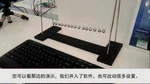
| CMOS (complimentary metal-oxide semiconductor) imaging technologies arrived on the scene about the same time as CCD (charge-coupled device) imagers. However, it has been only within the last decade that CMOS imaging has started to rival that of CCD. Both are widely used in machine vision, but users still debate which technology is best.Each technology tends to satisfy basic needs for the majority of machine-vision applications. CCDs create higher image quality, produce better signal-to-noise ratios, and possess greater reproduction repeatability. On the other hand, CMOS imagers usually cost less, consume less power, and make for smaller systems. While CCD imagers work by photon capture (see last month’s Sensor Sense), CMOS imagers typically use a photosensitive diode or transistor that changes conductivity when struck by light. Each lightsensing element, or photosite, needs a corresponding electronic control circuit to read the amount of light striking it. The circuit usually contains a charge-to-voltage converter, a sample-hold system, noise-correction circuits, and multiplexers to synchronize and sequence the photosite output with all of the other photosites on the imager. With all their control circuitry residing on the same silicon wafer, CMOS imagers typically do not need the kind of external electronics that supports CCD imagers. However, CMOS control circuitry is complex. Compared to a comparable CCD chip, the CMOS device has less area available for light capture. Often its light-sensitive area is less than 25% of the imager’s total surface area. This is one reason CMOS may not be the first choice where low light levels predominate. The photon-capture ability of CCDs performs an integration role to deliver a more-robust image with low light levels. Some CMOS imagers have a collection of tiny lenses, called a microlenticular array, that covers the entire surface. The array focuses light gathered over larger areas onto the sensitive photosites to boost capture area and improve light sensitivity. Finally, CMOS may not be the best way to see supersmall features. CCDs work better where the geometries of the feature under inspection need subpixel (typically less than 7-μm) accuracy. |